

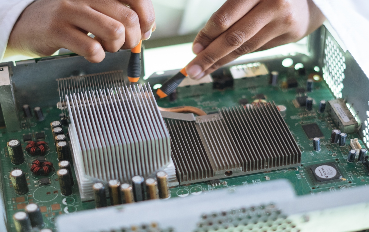
Researchers at the Indian Institute of Technology in Bombay (IIT-Bombay) have invented the first-ever indigenous semiconductor memory technology that can be adapted for manufacturing at the commercial unit of 180nm node in India. The technology enables secure memory and encryption hardware.
A recent news report explained that memory is a critical aspect of the internet-of-things (IoT), a network of objects embedded with sensors or chips for the exchange of data over a wireless network. Memories are used to customise chips by giving them user-specific storage of digital data. IoT connects tiny chips, which are all identical but distinguished by an identity (a barcode) stored in the memory. This data is stored within metal-insulator-metal (MIM) memory cells on a silicon integrated circuit memory chip.
The team invented the one-time programmable (OTP) memory-based technology on ultra-thin deposited silicon dioxide (a few atoms thick) instead of the existing gate oxide-based OTP technology. In contrast to the high voltage required by gate oxide breakdown (a popular OTP memory), IIT-Bombay’s memory chip uses less power and chip-area as the need for boosted voltage supply is avoided.
The project was initiated by the Department of Science and Technology’s (DST) Intensification of Research in High Priority Area (IRHPA). Aspects of the work were funded by DST’s Nanoelectronics Network for Research and Applications (NNetRA), DST-Advanced Manufacturing Technologies, and the office of PSA for hardware security. The team at IIT-Bombay partnered with IIT-Delhi, SETS Chennai, and Defence Research and Development Organisation for hardware encryption.
At a time when IoT is disrupting the semiconductor industry worldwide, the semiconductor manufacturing ecosystem led by Semi-Conductor Laboratory (SCL), Mohali, under the Department of Space, had to import the technology from abroad. SCL is the most advanced semiconductor manufacturing fab (a large facility with cleanroom environments used to produce memory chips) in the country. SCL aims to create a strong research and development base in the country in the field of microelectronics. The lab design and development of devices in cutting-edge technology and to transform SCL as a Centre of Excellence in Microelectronics in the country.
The team of researchers, along with SCL, successfully demonstrated a complementary metal-oxide-semiconductor (CMOS)-180nm-based 8-bit memory technology. The technology is adopted for production, the report added. Ideally, silicon chips (like thermometers) should be identical, but manufacturing variations produce tiny offsets (such as errors in temperatures), which are revealed upon testing. This renders a large fraction of chips useless. The technology designed by the IIT-Bombay team enables storing this offset correction in memory once and applying it to the output afterward to make each imperfect chip perfect. Using this method, generic chips can now be designed and make application-specific offsets added to make expensive custom chip design redundant, saving time and money for the user.
The global semiconductor market is expected to expand by 25.1% this year, according to a report. The market is expected to grow to US$551 billion in 2021, up from its previous forecast of US$527.2 billion. It expected the growth rate of the memory chip market to reach 37.1%, followed by analogue semiconductors with 29.1% and logic chips with 26.2%. The report predicted all regions to post double-digit growth this year, with the Asia-Pacific area leading the growth at 27.2%. Europe was the runner-up with 26.4% followed by the Americas with 21.5%.