

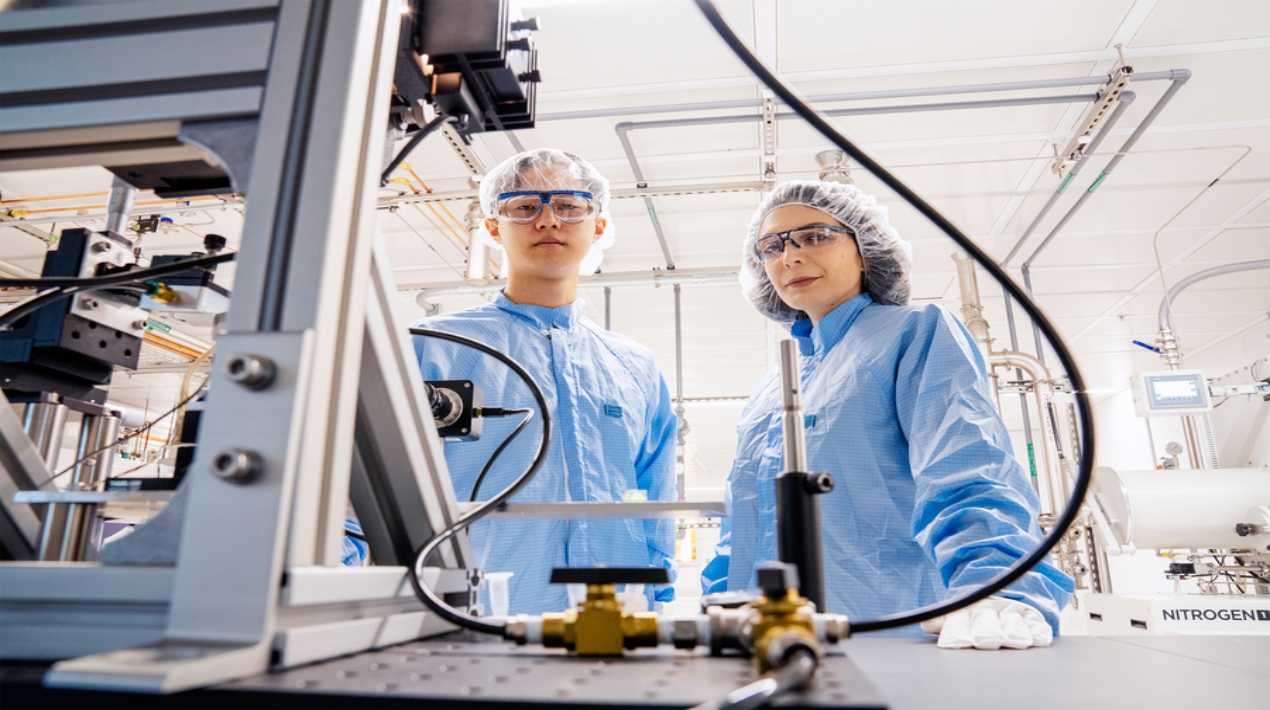
The Massachusetts Institute of Technology (MIT) researchers have created a method for precisely arranging and positioning nanoparticles on a material, such as the silicon used in computer chips, without harming or contaminating the surface of the substance.
The method, which combines chemistry and directed assembly processes with traditional fabrication techniques, makes it possible to efficiently form high-resolution, nanoscale features that are integrated with nanoparticles for devices like sensors, lasers, and LEDs, which could improve their performance.
To get the appropriate arrangement of nanostructures, materials are often etched away to create transistors and other nanoscale devices. The smallest nanostructures, however, are difficult to make at scale and with the required precision, require expensive equipment, and can enable the highest performance and new features.
The bottom-up assembly is a more accurate method for creating nanoscale devices. One method involves using chemistry to “grow” nanoparticles in solution, dropping that solution onto a template, organising the nanoparticles, and then transferring them to a surface.
But this method also has significant drawbacks. The template must first be effectively used to organise thousands of nanoparticles. Additionally, applying them to a surface frequently involves the use of chemical adhesive, intense pressure, or high temperatures, all of which have the potential to harm the surfaces and the final device.
To get over these restrictions, the MIT researchers created a fresh strategy. They efficiently arranged particles in the appropriate pattern using the strong forces that occur at the nanoscale and then transferred those particles to a surface at lower temperatures and without the use of chemicals or high pressures. These nanoscale structures can be inserted into parts for electronic and optical equipment, where even minute flaws can impair performance because the surface material is still flawless.
The researchers employ chemistry to make nanoparticles with a specific size and form in a solution to start their creation process, which is referred to as nanoparticle contact printing. Scientists then create a template in the form of a flexible surface covered in guides or traps that are the size of nanoparticles and are organised in the shape they desire for the nanoparticles to take.
They begin by putting a drop of the nanoparticle solution into the template, and then they employ two nanoscale forces to place the particles. The nanoparticles are subsequently applied to any surface.
For forces to combine to organise the particles, the researchers create template guides that are precisely the right size, shape, and arrangement. Then, without using any solvents, surface treatments, or high temperatures, the nanoparticles are printed onto the surfaces.
This results in yields of over 95% while maintaining the surfaces’ cleanliness and characteristics. Using this method, the team was able to arrange nanoparticles into any patterns, such as alphabetic letters, before precisely transferring those shapes to silicon. The technique also functions with nanoparticles of other shapes, such as spheres, and with several kinds of materials.
It is capable of efficiently transferring nanoparticles onto a variety of surfaces, including flexible substrates for the next generation of electrical and optical structures and devices as well as gold. Additionally, because their method is scalable, it can be expanded to be applied to the production of actual devices.