

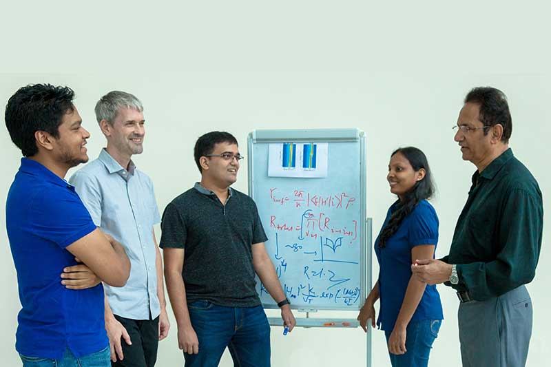
Above photo: Researchers from the National University of Singapore (NUS) led the invention of a novel organic resistive memory device that is cheaper and has higher endurance as well as better energy efficiency than commercial flash memories. The overall coordinator for the project is Professor T Venky Venkatesan, Director of NUS Nanoscience and Nanotechnology Institute (extreme right). / Credit: National University of Singapore
An international research team led by scientists from the National University of Singapore (NUS) pioneered the development of a novel thin, organic film that supports a million more times read-write cycles and consumes 1,000 times less power than commercial flash memories.
The organic film can store and process data for 1 trillion cycles and has the potential to be made even smaller than its current size of 60 square nanometers, with potential to be sub-25 square nanometres.
Professor T Venky Venkatesan, Director of NUS Nanoscience and Nanotechnology Institute (NUSNNI), the overall coordinator for this groundbreaking project said, "The novel properties of our invention opens up a new field in the design and development of flexible and lightweight devices. Our work shifts the paradigm on how the industry has traditionally viewed organic electronics, and expands the application of such technologies into new territories."
The invention of the memory device was first reported online in the journal Nature Materials on 23 October 2017.
Today we rely on ubiquitous silicon-based flash memories to store the massive volumes of data being generated. For years, the computer industry has sought to develop memory technologies with higher endurance, lower cost, and better energy efficiency than commercial flash memories. However, the industry has not used organic systems in memories due to limitations in performance, questionable claims of reproducibility, and the lack of scientific clarity on mechanisms through which they exhibit their behaviour.
Addressing these challenges, Mr. Sreetosh Goswami, a researcher from NUSNNI and a graduate student from the NUS School of Integrative Sciences and Engineering working under the supervision of Prof. Venkatesan, successfully fabricated an organic resistive memory device that outperforms commercial flash memory in terms of endurance (Write endurance is the number of program/erase cycles that can be applied to a block of flash memory before the storage media becomes unreliable), energy efficiency and cost. He developed 600 working devices which demonstrated impeccable reproducibility.
According to Mr. Goswami, this is the first time that an organic device is looking industrially competitive. "Also, we have developed a clear picture of the molecular mechanism based on our in-situ studies which organic devices have always been lacking," he added.
The new device utilises a transition metal complex[1] which was designed and synthesised by Professor Sreebrata Goswami and his team, comprising graduate students Mr. Santi Prasad Rath and Mr. Debabrata Sengupta, from the Indian Association for Cultivation of Sciences.
Based on understanding of a unique family of metal complexes, acquired over a few decaded, Prof. Goswami and his team are now able to engineer new materials by bring together different variations in the molecules, adding active functions and using right counter ions.
In order to understand the science behind the device performance, Prof. Venkatesan established a collaboration with Professor Victor Batista from Yale University. Besides simulating the spectral behaviour of the molecules, Dr. Svante Hedstrom and Mr. Adam Matula, who are from Prof Batista’s team, were able to identify the role of the counter ions in the molecule which gave rise to a non-volatile memory behaviour.
Prof. Batista explained that the counter ions surrounding the molecules act like the ratchets on a wrench, and offer stability to the various electronic states of the molecule which are necessary to achieve the memory effect. This molecular-level understanding is unprecedented in a memory device, and will allow the creation of design principles for the next generation of devices
Industry applications
The research team is planning to partner a consumer electronics company to commercialise the new technology. In addition, the researchers are also looking at fabricating multi-state memories to produce neuromorphic memory devices[2] (that resemble the brain) for artificial intelligence (AI) applications, one of the fastest growing technology fields today.
Prof. Venkatesan elaborated, "AI relies on neuromorphic computing to simulate the architecture of the human brain. Therefore, the development of neuromorphic memory devices that can embody the concept of learning endemic to biological memory is crucial. Given the success of our current work, I believe we are on the right track to fabricate innovative memories which will have more than two states while maintaining all the fascinating properties of the device we currently have."
[2]As this Wired article explains: “Traditional CPUs process instructions based on “clocked time” – information is transmitted at regular intervals, as if managed by a metronome. By packing in digital equivalents of neurons, neuromorphics communicate in parallel (and without the rigidity of clocked time) using “spikes” – bursts of electric current that can be sent whenever needed. Just like our own brains, the chip’s neurons communicate by processing incoming flows of electricity – each neuron able to determine from the incoming spike whether to send current out to the next neuron.” The idea has been there since the 1980s. But they haven’t yet moved from research labs to commercial applications. Neuromorphics could enable deep learning application right inside a mobile phone. Today, deep learning enables many widely used mobile features, such as the speech recognition required when we ask Siri a question. But the actual processing occurs in the cloud. The mobile device does not have sufficient computing power. That could change with neuromorphics.